Category Archives: TechNews

Hacker Attacks on Crypto Protocols: Nearly $500M in Damage Last Quarter

Image: Hacker, Free Stock Picture, MorgueFile.com.

As the company Atlas VPN has found, hacker attacks have been particularly successful in recent months. Chainalysis had already warned of a record month.

Although the cryptocurrency sector is now much better regulated and more and more investors are taking the necessary steps to increase security – such as storing their own coins in hardware wallets – hacker attacks are still a big issue in the cryptocurrency sector, albeit only in relation to the volume traded affect a fraction of the sector.

In one quarter, hackers cause almost half a billion dollars in damage

According to Atlas VPN data , in the third quarter of 2022, criminals stole around $483 million worth of cryptocurrencies through targeted attacks. The number of hacks fell by 43 percent compared to the second quarter. In the first quarter, the damage amounted to around 1.3 billion US dollars.

Even if the damage appears large in absolute numbers and was certainly significant for those affected, in relation to the size of the crypto sector with a value of around $970 billion according to CoinMarketCap, it is not quite as dramatic as it might seem at first glance.

Ethereum, Polkadot and BNB Chain particularly affected

The hacks primarily affected the Ethereum network. A total of 11 attacks on Ethereum blockchain-based protocols caused $348 million in damage. However, considering that most protocols run on Ethereum, this is not surprising. For Polkadot, it was $52 million in just two attacks. While projects on the BNB chain have been attacked 13 times, the damage amounts to only $28 million.

It is important here that the blockchains themselves are not attacked. Instead, it is mainly smart contracts in the DeFi area that cause security gaps.

This quarter could be a record

Chainalysis also deals primarily with the damage caused by cybercrime in the cryptocurrency sector. The figures determined by Atlas VPN for the third quarter correspond to the information from Chainalysis, which expects a record month for October. As Chainalysis announced on October 12, eleven hacker attacks with damage totaling $718 million had already been registered by then.

If the trend of the month continues, the fourth quarter is likely to be the most momentous for the cryptocurrency sector. The BNB chain hack caused a stir this month , in which at least no funds were stolen from other users. Instead, the attackers created over $100 million worth of coins out of thin air.

PS5 hacked: modder with surprising discovery

Image: Hacker, Free Stock Picture, MorgueFile.com.

After a jailbreak on the Playstation 5 was successful at the beginning of the month, a modder has now published his first finds. They provide clues to the great mysteries of the gaming scene.

A so-called jailbreak describes the state when the settings of a device are “liberated” by a hack and thus become freely accessible and variable. This is exactly what was recently achieved on the Playstation 5 .

Lance McDonald, the modder who achieved this feat, has now dug deep into the game console’s file archive – and discovered some amazing things, as the online magazine Eurogamer reports.

Legendary hoax ring suddenly real

The first thing that the digital treasure hunt brought to light is actually a legendary treasure from the gaming scene. In the files of the Demon’s Soul remake, McDonald found a 3D model of the legendary Chieftain’s Ring.

The supposedly powerful artifact was originally a hoax from fans in the original game. Fake screenshots and eyewitness accounts claimed the item’s existence, leading players to frantically search for the item in-game – even though it never existed.

So that could change in the remake – a friendly wink from the programmers to the fan base.

“Abandoned” a secret “Silent Hill” project?

McDonald’s second find is no less mysterious: he found a file directory for the game “Abandoned” – a survival horror game from the studio Blue Box – which was initially widely announced and then suddenly disappeared from the scene completely. In addition, the developer studio published contradictory statements, which were then deleted.

It is not known whether the strange behavior is a marketing strategy. However, the files contain references to consciously playing with gaming myths. Because in the “Abandoned” folder there is a map called PT2 – an allusion to the never completed “Silent Hill” successor.

“Seems like at some point they planned to have some ‘this is secretly a silent hill project’ bullshit trail up their sleeves,” the modder wrote on Twitter.

With these interesting finds, one can remain curious as to what else McDonald will find in the cracked heart of the PS5.

iPhone 14 Pro chip bigger despite smaller transistors

Image: Circuit Board, Free Stock Picture, MorgueFile.com.
Closeup of old circuit board. Image: Circuit Board, Free Stock Picture, MorgueFile.com.

Small changes to caches and processor cores, this is how a preliminary analysis of the A16 silicon chip  from Angstronomics can be summarized. Although there is still no high-resolution image of the die, there is a video in which some details can already be seen. Since various components such as caches, processors and GPU form unique patterns on the die, they can be identified and at least roughly measured.

The operator of Angstronomics, who publishes under the pseudonym Skyjuice, comes to the conclusion that Apple has reduced the L3 or system level cache (SLC) in the A16 compared to the predecessor A15. Compared to the 4 MB L2 cache of the Efficiency CPU cluster made of Sawtooth cores, each of the two SLC blocks occupies about three times the area, so it should hold 12 MB – the SRAM memory cells need the same regardless of the cache hierarchy lots of space.

This means that the SLC of the A16, at 24 MB, is a quarter smaller than that of the A15, which has 32 MB. However, Apple has given the performance cores named Everest a third more L2 cache: the area here suggests that each of the two blocks holds 8 MB, while the A15 had a total of 12 MB.

One can only speculate about the reason for the reduction of the size of the SLC: Angronomics brings the higher data rate of the memory into play as a possible reason: LPDDR5-6400 is used for the first time in the A16. Optimizations are also conceivable, since the L2 cache of the P-cores was enlarged at the same time. Many factors play a role in the dimension of caches, including the micro architecture of the processors – it is very likely that there was not a single decisive argument for the redistribution.

Changes to processor cores

There are also small changes in the processor cores: they are arranged differently on the die, and Apple has also revised their structure. Both the Everest and Sawtooth (P/E) cores also appear to be slightly larger than their Avalanche and Blizzard predecessors. The neural and graphics processing units (NPU and GPU), on the other hand, seem to be quite unchanged. However, they are hardly recognizable in the Angtronomics image.

However, the NPU is only eight percent faster than the A15. This is part of the switch from the supplier TSMC from the N5 to the N4 process and the expected increase in speed of ten percent as a result. Major changes are therefore unlikely. The higher switching speed of the transistors in N4 should also play a role in the GPU, which also benefits from the larger memory bandwidth. Together, both could almost explain the measured 28 percent increase in speed .

Bigger chip despite (slightly) smaller transistors

With N4, TSMC refers to a further development of the N5 manufacturing process, with which Apple’s A15 is manufactured. According to TSMC, this increases the integration density by six percent, and the number of transistors also increases by six percent – ​​16 billion in the A16, 15 billion in the A15. Theoretically, the dies of A15 and A16 could be the same size.

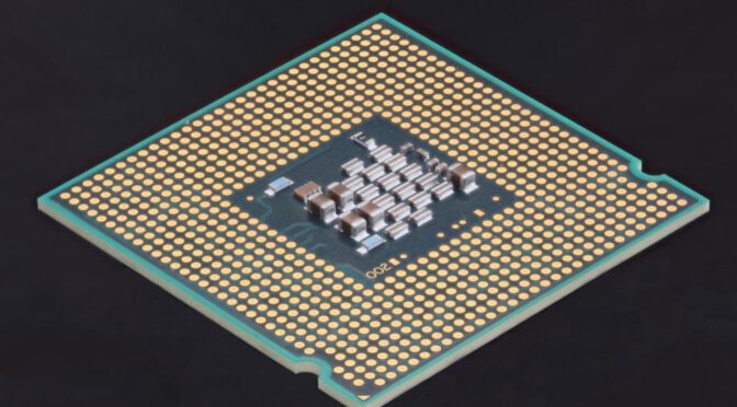
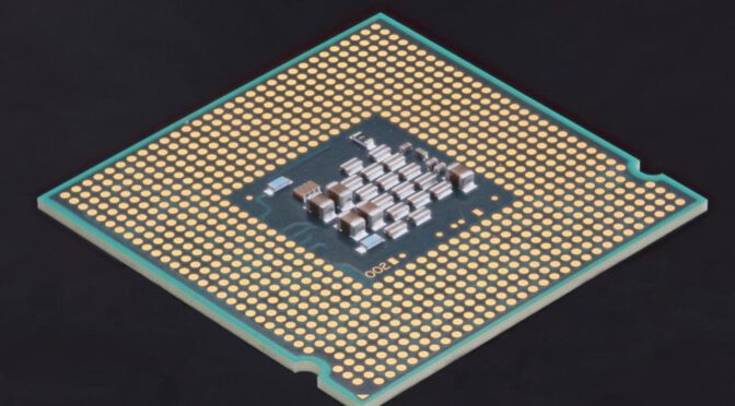
Intel discontinues Pentium and Celeron for new Intel processor

Image: Intel, Free Stock Picture, MorgueFile.com.

Intel is set to retire its long-used Pentium and Celeron CPU brands and has instead opted for a new, unified naming structure for Intel processors.

Starting in 2023, Intel notebooks will be powered by an Intel processor that spans multiple processor technology families.

“Intel is committed to driving innovation for the benefit of users, and our entry-level processor families have been instrumental in raising the standard of PCs at all price points,” said Josh Newman, the company’s interim general manager of Mobile Client Platforms.

“The new Intel processor branding will simplify our offering so users can focus on selecting the right processor for their needs.”

An Intel Pentium chip was first used in a consumer PC in 1993, and many generations have come since then. The Celeron chips were introduced in 1998.

Intel is looking to simplify the entire naming structure, with “Intel Processor” set to join the flagship Intel Core, Intel Evo, and Intel vPro brands.

The idea behind this change is to make it easier for consumers to buy products. However, mostly only the branding will change, since the product lines that the chipmaker plans to serve remain largely the same.

Adobe buys Figma

“The merger of Adobe and Figma will herald a new era in collaborative creativity,” Adobe said in a statement on the multi-billion dollar deal.

The US software manufacturer Adobe has announced the acquisition of Figma. In the morning of September 15, the news site Bloomberg initially announced a potential deal. Citing insider information, followed a little later by official statements from Adobe and Figma .

Image: Financial, Free Stock Picture, MorgueFile.com.

Figma and Adobe: These are the details of the deal

Figma is a platform for collaborative web design. It was previously considered more of a competitor program to Adobe. Now the company is being transferred to the software giant’s portfolio for around 20 billion US dollars. Part of the purchase price will be paid by Adobe in shares. It is the largest known deal in the history of the software manufacturer.

“The merger of Adobe and Figma will usher in a new era of collaborative creativity,” Adobe says, and: “Figma’s web-based multiplayer capabilities will accelerate the delivery of Adobe’s Creative Cloud technologies on the web and make the creative process more productive and make it accessible to more people.”

However, it will probably take a while before the deal is finalized: on the one hand, Figma’s shareholders have to agree to the takeover, and on the other hand, official approvals are required. Adobe expects to close in 2023, by which time the two companies would “continue to operate independently.”

Figma co-founder remains CEO after Adobe acquisition

According to Dylan Field, co-founder of Figma, there will not be a radical change in leadership: “Adobe is determined to continue operating Figma independently, and I will continue to act as CEO and report to David Wadhwani.” Wadhwani is Chief Business Officer of Figma Digital Media at Adobe.

Field also writes about the acquisition: “We have a great opportunity to accelerate the growth and innovation of the Figma platform with access to Adobe’s technology, expertise and creative resources.”

Some things would remain the same for the time being – for example the pricing. Since it is known “that we are in an unpredictable, inflationary environment”, no price changes are currently planned. “And finally, Figma will continue to be free for educational purposes” – that was a crucial part of the negotiation talks with Adobe.